Transistors were invented by J.Bardeen and W.H.Brattain of bell laboratories in USA in 1947 and that was a point contact transistor.
William shockey first invented junction transistor in 1951 which consists of two back to back p-n junctions.
These transistors are also known as bipolar junction transistor (BJT) and are our subject of study in this section.
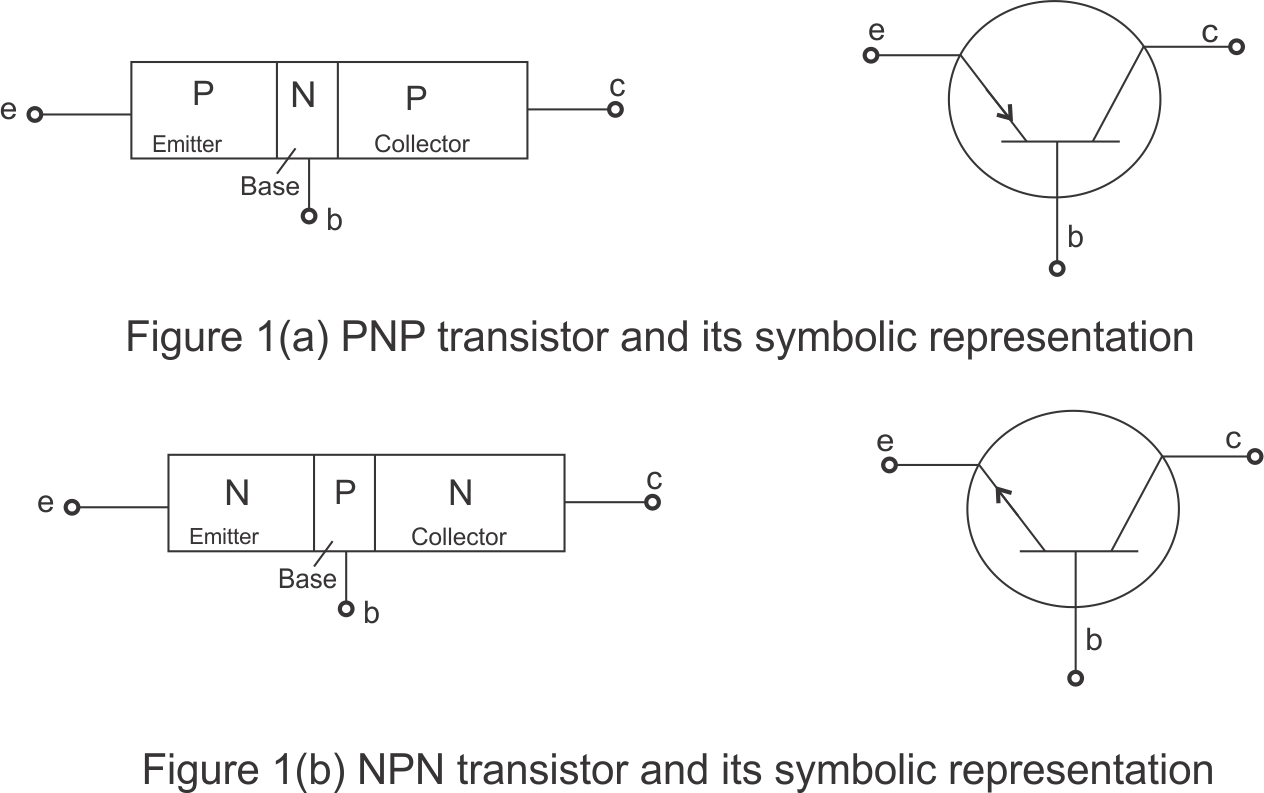
Thus a junction transistor is formed by sandwiching a thin layer of p-type semi-conductor between two layers of n-type semi-conductor and vice versa.
Transistors are of two types
PNP transistors : Here the n-type thin layer is sandwiched between two p-type layers
NPN transistors : Here p-type thin layer is sandwiched between two n-layers
There are three regions in a transistors
emitter
base
collector
Figure (1) shows diagrammatic representation of PNP and NPN transistors along with the symbols used to represent them
All the three regions of the transistors have different thickness and their doping levels are also different.
In symbolic representation of transistors the arrow head shows the direction of conventional current in the transistor.
Brief description of all the three region of the transistors
Emitter: Emitter region of transistor is of moderate size and it is heavily doped .Function of emitter is to inject electrons or holes depending on types of transistor into the base
Base: Middle region of transistor is known as base region.This region of transistor is very thin and very lightly doped.Function of the base is to pass most the electron or holes onto the collector
Collector: Collector region is moderately doped and is made physically larger than the emitter since it is required to dissipate more heat .Collector has a job of collecting electrons or holes from the base.
Action of transistor
Transistor has two junctions
Emitter base (EB) junction
collector base(CB) junction
To operate the transistor a suitable potential difference must be applied across two of its junction .This is known as biasing of the transistor
The charge carriers move across different region of the transistor when all three terminals of transistors are properly biased
There are four possible ways to bias these functions given below in the table
Condition
EB junction
CB junction
Region of operation
1
FB
RB
Active
2
FB
FB
Saturation
3
RB
RB
cut off
4
RB
FB
Inverted
Only one of these conditions interests us at the moment that is condition 1 in which EB junction is FB and CB junction is RB
We will consider the case of npn transistor when its EB junction is FB and CB junction is RB.Case of pnp transistor can be also be understood on the same basis
the figure 2 shows that an npn transistor is properly biased using the two power supplies VEE and VCC and base terminal is common to both these power supplies
Consider figure 2a ,since emitter base terminal is FB the majority charge carriers there are electrons in this case enters the base region in large numbers
Base region which is very lightly doped is short of majority charge carriers which are holes in case of npn transistors.Since base is a p-type semiconductor ,thus large numbers of electrons entering the base from the emitter combines with the very small number of holes present there in base region
Since the base collector junction is RB so these electrons which are minority charge carriers in base ,can easily cross the junction and enter the collector region
These electron just entered the collector region moves forwards to reach the collector terminal
These electron go through batteries Vcc and VEE and are taken back to emitter
The electrons going from source VEE to emitter constitute the electric current IE in the direction opposite to the direction of the flow of electron .This current is known as emitter current.
Similarly electron moving from the collector to the battery constitute the collector current IC
Collector current IC is slightly less then that of emitter current IE because some of the electrons comes out of the base terminal instead of going to the collector
This small fraction of current coming out of base terminal is known as base current IB.Base current is a small fraction of the emitter current
Using Kirchhoff's Rules we can write
IE=IC+IB ---(1)
There is always a reverse leakage current in the transistor which is due to the movement of minority charge carriers
α and β parameters for transistor are defined as
α=IC/IE
β =IC/IB ----(2)
These parameters are helpful while analysing transistors as a circuit element
We have to keep one connection in mind that all currents entering into transistor are taken to be positive and current flowing out is negative
Thus for an NPN transistor
IE -> negative
IC ,IB-> positive
Transistor circuit configuration and transistor characteristics
There are three terminals in the transistor i.e emitter,base and collector
In circuits input and output connections are made such that one of the terminals of the transistor is common to both the input and output
Keeping this in mind ,transistor can be connected in any of the three following configuration
Common emitter configuration(CE)
Common base configuration(CB)
common collector configuration( CC)
In all these configurations voltage connection are made such that EB junction is always forward biased and CB junction is always reverse biased so that transistor works in the active region
Out of all the three transistor configuration CE is most widely used so our discussion would be restricted to this configuration only
Common Emitter transistor configuration
In CE configuration emitter is made common to both input and output or the input is between the base and emitter and output is between emitter and collector.
Figure below shows an transistor circuit using npn transistor in CE mode
Input section of the circuit contains base emitter base junction .Thus two input variables are
IB ,the base current
VBE ,the voltage in the input section
Similarly output section of the circuit contains CE junction .Thus two output varibel are
IC ,the collector current
VCE ,the collector emitter voltage
Transistor characteristics are the curves that relate transistor currents and voltage .There are two types of characteristics curves
Input characteristics :- relates input current with the input voltage for a given output voltage
Output characteristics :- relates output current with output voltage for a given input current
We now know what are transistor characteristics and now we shall discuss the characteristics curves for a npn transistor in CE configuration (connection shown in above figure)
(i) Input characteristics:-
To study input characteristics of transistors in CE configuration a curve is plotted against base current IB and base emitter voltage VBE keeping collector emitter voltage VCE fixed
Input characteristics relate IB and VBE for different values of VCE
Graph below shows the input characteristics of npn transistor which are similar to those of a forward biased pn junction
Change in output voltage VCE does not result in large deviation of the curves
To keep transistor in active state ,it is required to keep VCE large enough to make CB junction reverse biased
Dynamic resistance of the transistor at a given VCE is
ri=ΔVBE/ΔIB
for VCE=constant ---(3)
input resistance ri is defined as the ratio of change in base emitter voltage (ΔVBE) to the resulting change in base current (ΔIB) at constant CE voltage(VCE)
Value of ri can vary from few hundred to few thousand ohms
(ii) Output characteristics:-
These curves relate output current IC to the voltage between collector and emitter for various values of the input current IB
Output characteristics are shown below in below figure
In active region ,IC increase slowly as VCE increases
From output characteristic we can determine dynamic output resistance which is defined as the ratio of the change in CE voltage (ΔVCE) to the change in collector current (ΔIC) at a constant base current IB
Thus,
ro=ΔVCE/ΔIC
for IB=constant ---(4)
current amplification factor (Β) is defined as the ratio of change in collector current to the change in base current at constant CE voltage
=> Βac=ΔIC/ΔIB at VCE=constant ---(5)
Βac is also known as ac current gain
Simple ratio of IC and IB is known as DC current gain.Thus
Βdc=IC/IB ---(6)
From fig (5) it is clear that for constant IB ,current IC increases with VCE. This indicates that Βdc increase with VCE
When VCE drops below VBE,the CB junction becomes forward biased and IC decrease rapidly with VCE
is
When both junctions are FB ,transistors works in saturation region in this region IC no longer depends on IB
Inactive region collector region is Βdc times greater than IB.This shows that small input current IB produces large output current IC