Main utility of a transistor lies in its ability to amplify weak signals
An amplifier is a circuit which is capable of increasing the signals and a transistor can not accomplish this task.
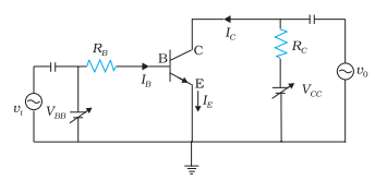
Along with transistors an amplifying circuit consists of passive components like resistors and capacitor and a biasing battery
We generally use CE configuration of transistor for most of amplifier circuit as it has high current voltage and power gain. Also input and output impedance characterstics of CE type amplifier are suitable for many applications
Figure given below shows the basis CE amplifier circuit using an NPN transistor
The Battery VBB forward biases the emitter junction and the collector junction is biased by battery VCC relatively higher voltage battery then VBB
Role of load resistance RB is to limit the base current within certain specified limits and RC is the load resistance in the collector circuit and amplified AC voltage appears across it.
The emitter terminal is common and grounded
In this common emitter circuit the input signal is applied to the base and output signal is obtained at the collector
We know that very small base current in a transistor corresponds to large collector current
Therefore with input signal applied to the base, a very small charge in IB produces a much large change in IC and thus a substantial current gain is obtained
The potential difference VBE changes with time due to the alternating input signals and this leads to the change in base current
In the absence of ac signal a closed emitter base circuit results IB,IE and IC as base ,emitter and collector currents .From Kirchhoff first law
IE=IB+IC ----(7)
Due to collector current IC a voltage drop develops across RL which is equal to ICRL
Applying Kirchhoff�s law in output loop we get
VCC=VCE+ICRC ---(8)
and for input loop we get
VBB=VBE+IBRB ---(9)
when input signal vi is not zero then
VBB+ Vi=VBE+IBRB +ΔIB(RB+ri)
where ri is the input dynamic resistance relating VBE and IB as given in equation (3).Hence
vi=ΔIB(RB+ri)=rΔIB
The change in IB causes a change in IC. Thus AC current gain Ai (or Βac) is defined as
Βac=ΔIC/ΔIB=iC/ib ---(10)
Change in collector current IC due to change in IB causes a change in VCE and the voltage drop across RC as VCC is fixed
Thus from equation (8)
VCC=VCE+ICRC
so ΔVCC=ΔVCE+ΔICRC
as ΔVCC=0
Or
ΔVCE=-RCΔIC
This change in VCE is the output voltage ,Thus
v0=ΔVCE=-RCΔIC
=-ΒacRCΔIB
Voltage gain for the amplifier is
Av=v0/vi=ΔVCE/rΔIB=-ΒacRC/r ---(11)
Here negative sign in equation (11) represents that the phase of the output voltage is opposite to that of input voltage
Power gain of the amplifier is given by
Ap=ΒacAv=Βac2RC/r ---(12)