Conducting materials or conductors are good conductors of electricity for example aluminium ,copper,silver etc. where as insulating material or insulators are bad conductor of electricity for example porcelain,glass,rubber etc
Apart from conductors and insulators,there are another group of materials such as germanium or silicon which are neither good conductors nor good insulators
These materials such as silicon and germanium are known as semiconductor and have conductivities fairly lower then that of conductors and much higher then that of insulators at room temperature
Thus semiconductor materials have electrical properties lying in between those of insulators and good conductors
Semi conducting materials have negative temperature coefficient of resistance which means that conductivity of semiconductor increases with temperature unlike the case of conductors where resistivity of the materials increases with the increase of the temperature
Conductivity of semiconductors can also be controlled by the addition of impurities which we should study later in this chapter
Atomic structure
An atom consists of a positively charged core known as nucleus and a number of negatively charged particles called electrons round the nucleus in fixed circular or elliptical orbits
This positively is made up of two subatomic particles namely protons and neutrons out of which protons are positively charged particles and neutrons are electrically neutral particles
Mass of neutrons is nearly same as that of proton
Almost all the mass of the atom is concentrated in the nucleus
electrons revolving round the nucleus are relatively lighter particles with weight nearly 1040 times less then a proton ( or a neutrons)
An electron and proton both contain same amount of charge but as we know earlier electron are negatively charged and proton are positive charged particles
In a normal state atom is electrically neutral which means that in an atom number of electrons orbiting round the nucleus must be equal to number of protons in its nucleus
The number of protons in an atom is called its atomic number
All the electrons in an atom does not move in a same orbit rather they are arranged in different orbits or shells
In general ,a shell can contain a maximum number of 2n2 electrons where is the no of the shell.So first shell contain maximum of 2 electrons.second cannot contain more than 8 electrons and so on
electrons present in outermost orbit are called valence electrons
Free electron model of the atom and energy band's in solids
we already know that electrons present in outermost orbit of a atom are valence electrons
The coulomb force due to the nucleus on these valence electrons is almost negligible
Generally solid posses crystalline structures and the atoms in solid are arranged symmetrically in regular manner
Due to negligible amount of coulomb interaction between valence electrons and nucleus of atom,these valence electrons are not bound with a particular atoms in the crystal lattice of the solid
These valence electrons also known as free electrons freely move in zigzag path moving anywhere in the crystal
These free electrons are bound as a whole with the crystal or solid which means they do no posses sufficient energy to cross the surface of the solid and came out of it
Each isolated atom has only a certain number of orbits available and these available orbits represent the energy levels for the electrons
Quantum theory tells us that only few specific discrete value of electron energy are possible
An electrons can not any value of the energy and no electron can exist at a energy level other than a permissible value
The space between allowed energy levels or states is forbidden region and electron cannot stay there as those electron energy is not allowed according the quantum theory
Hence there are specific energy states in an atom and electrons can occupy those states only
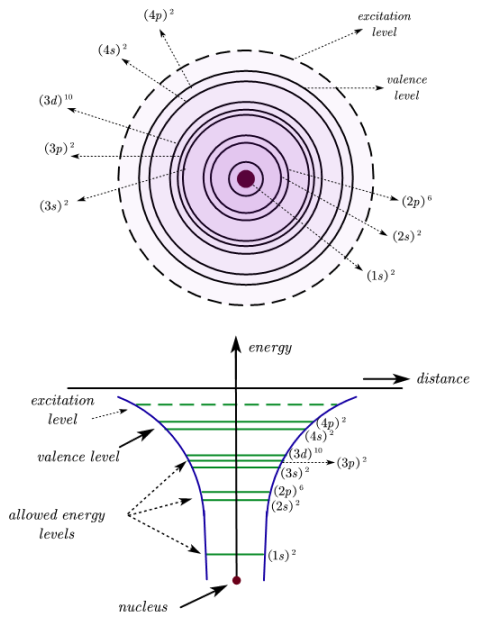
Figure given below shows germanium atom and its various energy states
First three states (along with their sub states) of germanium atom are completely filled buts its outer orbit is not filled completely as there are two electron each in both sub states of this outermost state
These four electron in outermost orbit of germanium atom are valence electrons and they are in 4s2,4p2 sub shells and these shells are called valence shells
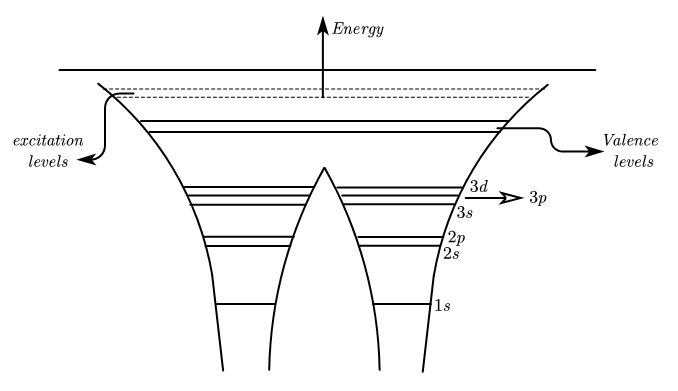
When two atoms of a solid are brought close to each other ,then their PE curves interact with each other due to which their energy states are slightly disturbed
Due to this interaction energy ,valence energy state divided into two sub energy states,one of them lie above the original energy state and another below it
The energy difference between these two states is so less that they are in the form of continuous band of energy .This is shown in figure given below
If there are N atoms brought together to form a crystal,they also interact in similar way as of two atom interaction diccused above
Due to interaction between N atoms,each energy level or states gets slightly disturbed and break up into N energy states
These two energy states lies on two sides of original energy states
Because of very large number of atoms in a crystal these newly developed energy levels are so close to each other that it is not possible to detect them individually'
Thus we can say that energy level of each atom takes the form of continuous band on interaction with other atoms in the crystal and they are energy bands in the solid
Figure given below shows that one dimension graph of energy levels when number of atoms are bought together so that their PE of one interact with the PE of the others
FIG
Energy band that is formed of valence energy levels of various atoms is called valence band and it is the band which consists valence electrons
energy band just above the valence band is called forbidden energy band and according to quantum theory ,electrons can not have energies equal to forbidden energy gap.Thus it is impossible to find an electrons in forbidden energy band
energy band just above the forbidden band is conduction band.Value of this band energy is equal to first excited state energy of the atom and excited electrons can be found into this band
Normally we do not find any electrons in the conduction band but if the electrons in valance band gain energy then on being excited with sufficient energy they goes to conduction band
An electron in a conduction band is completely free from the binding energy of the nucleus of the atom but the electron is still bound to the crystal lattice
Conductors,Insulators and semiconductor
We have already discussed about the formation of energy bands in solids
We also know that any material would be able to conduct only if it contains movable charges in it
These movable charges or free electrons that exists in the conduction band are able to move randomly inside the solid
In the presence of external electric field electrons get biased in the opposite direction to the of electroc field and can carry electronic charges from one point to another
There are some materials like metals that have excellent electrical conductivity ,there are materials that have extremely poor electrical conductivity which are known as insulators
Apart from conductors and insulators ,there are materials having their conductivities much greater then that of insulators and much lower than that of conductors and these materials are known as semiconductor
we will now classify these materials on the basis of their energy band structure
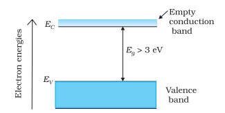
(i) Insulators
Figure given below shows the energy band structure of a typical insulators
As shown in the figure ,insulators have very wide forbidden energy gap (EG) nearly of the order of 3 eV or more
Because of this wide forbidden energy gap it becomes impossible for electrons present in valence band to cross the gap and reach to the conduction band and this makes electrical conduction a practical impossibility in insulators at room temperature
However at very high temperature or with very high voltage applied across the ends of insulators ,it may conduct and this is termed as break down of insulators
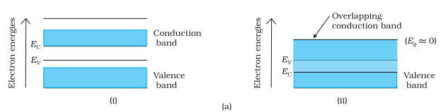
(ii) Conductors
Figure given below shows energy band structure of an typical conductor
As can be seen from the figure,conductor band and valence band overlap for conductors
Thus value of forbidden energy gap (EG) is zero for conductors and it does not exists at all
For metals or conductor ,valence band energies are same as the conduction band energies.An valence electron can very easily become conduction electron or( free electron) with out any supply of the heat energy
This is why metal contains large number of free electrons even at room temperature and are good conductors of electricity
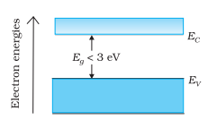
(iii) Semiconductors
Figure given below shows the energy band structure of a semiconductor materials
In semi-conductors forbidden energy gap has its value much less then that of an insulator .It has a value of the order of 1eV
Two most important semi-conductor used un semiconducting devices are silicon( EG =.785 eV at 0K) and germanium (EG =1.21 eV at 0K)
At very low temperature ,there is not much difference between an semiconductor or an insulator as both of them does not have any electron in their conduction band
However in case of semiconductors at room temperature ,due to thermal energy some electron manage to reach from valence band to conduction band and this makes semiconductors capable of conducting some electric current even at room temperature
This electric current flow in semi conductor at room temperature is much less then that of conductor
In the following section,you will learn about the conduction process in semiconductors
Intrinsic semiconductor
Semiconductor devices like diodes and transistors are made from single crystal of semiconducting material (silicon or germanium)
Semiconducting material in its pure from is called and intrinsic semiconductor
Atomic number of silicon is 14 and germanium is 32.So silicon has 4 valence electrons in its M-shell and germanium also has 4 valence electron in its N-shell
So both M-shell in case of silicon and N-shell in case of germanium are incomplete.So there are 4 valence electron of each silicon (Si) and germanium (Ge) around and internal core (nucleus + rigidly bound internal electrons)
To fill the valence shell each atom of Si(or Ge) require four more electron and this is done by sharing one electron each from the neighbouring atoms
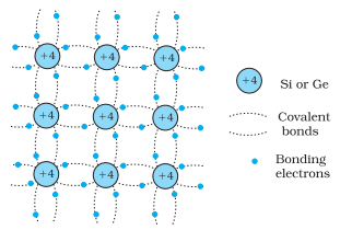
each of the atoms in silicon or germanium crystal arranged themselves in a uniform three dimension pattern so that each other atom is situated on corners of a regular tetrahedron.Such a pattern is called as crystal
Figure given below shows a simplified two dimensional representations of the crystalline structure of silicon ( or germanium)
here from the figure we see that +4 is the excess charge on the core of the Si(or Ge) atom as core of the Si atoms consists of 14 protons and 10 electrons and remaining four electron of atom are valence electrons shown around each core in above figure
each of the four valence electrons take part in forming covalent bonds with the neighbouring atoms
At absolute zero, valence electrons bound to their respective atoms and hence no free electrons are available for electrical conduction
This is the reason why semiconductor behaves like an insulator at absolute zero
at room temperature ,some of the covalent bonds break up and electron gain so much of the energy that they reach conduction band by crossing forbidden energy gap.This happens due to very low binding energy of covalent binding which easily breaks up with the increase in temperature
Due to this break up of the covalent bonding number of electrons n reaching conduction band is equal to the number of the electrons being released out of broken covalent bond
holes
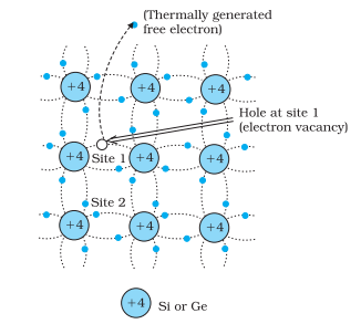
At absolute zero (T=0 Kelvin) a semi conductor behaves like an insulator but at room temperature some of the valence electrons of semiconducting material reaches conduction band and a vacant space is created in the covalent bond as shown in figure
These vacant spaces have a deficiency of negative charges and are called holes and these holes behaves like positive charges
In a crystal lattice these holes are free to move like free electrons inside the valence band
The moment electron breaks the covalent bond and moves to conduction band ,an electron hole pair is generated in the semiconducting crystal (Si or Ge)
In an intrinsic or pure semiconductor an electron hole pair generates as a result of thermal process as discussed above in other words we can say that in intrinsic semiconductor all free electron in conduction band are due to broken covalent bond and number of electron (nii
nii
Here subscript i represent intrinsic quantities
With the increase in temperature ,the number of free electron in Conduction band increases due to which conductivity of semiconducting material increases weight it
At room temperature semiconducting material has two types of charge carriers namely electrons in conduction band and holes in valence bond
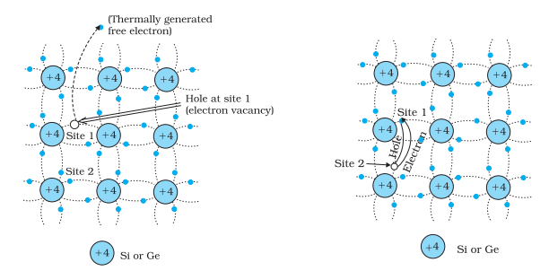
For understanding the movement of hole in semiconductor consider the figure given below
As can be seen from figure a thermally generated free electron creates a vacancy at site 1 thereby generating a hole. An electron from covalent bond at site 2 jumps to site 1 resulting a hole at site 2
This way hole moves from site 1 to site 2
Again electron from site 3 jumps to hole at site 2 generating hole at site 3 and site 2 has now electron
Here at site 2 process of recombination occurs as electron from site 3 recombines with hole at Site 2 generating hole at site 3
This way hole has now moved from site 2 to site 3
The electron which originally generated hole as a result of thermal process is not at all involved in motion of holes as thermally generated free electron has moved to conduction band and all this hole movement takes place in valence bond
This free electron which moved to conduction band moves independently as conduction electron and gives rise to conduction current Ie
On the application of electron potential across the crystal ,holes moves towards negative potential giving rise to hole current
In intrinsic semi-conductor current flow is due to electron in Conduction band and holes in valence band
Motion of holes is opposite but total current is equal to their sum as they are oppositely charged so,
Total current =I=Ie+ Ih
Ie : electron current
Ih : hole current
Extrinsic semi-conductor
Even at room temperature ,conductivity of intrinsic semi-conductor is very low and cannot be used for making suitable devices
Conductivity of the semi-conductor can be enormously increased if a suitable impurity is added to it in a very small proportion nearly 1:106 parts of pure semi-conductor
This process of adding impurity to a pure intrinsic semiconductor is called doping and a doped semiconductor is known as extrinsic semiconductor
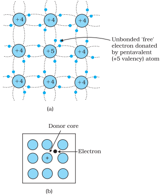
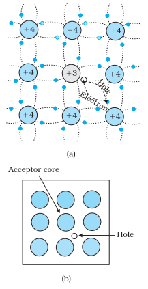
Usually doping agents (impurity) are pentavalent atoms having five valence electrons (bismuth,arsenic,phosphorous) or trivalent atom having three valence electron (gallium,indium,aluminium)
These doping material alters the structure of the semiconductor crystal as pentavalent impurities contribute one electron to the conduction band on intrinsic semiconductor and trivalent impurities accepts electron from the intrinsic semiconductor
Depending on the type of doping material used extrinsic semi-conductor are divided into two types
(i) N type semiconductor
(ii) P type
We shall now discuss about them in detail
N-type semiconductor
We already know that silicon or germanium atoms are tetravalent and have few conduction electrons at room temperature
If we dope a semiconductor crystal (Si or Ge) with pentavalent elements (antimony,phosphorous etc) in a very small amount then these pentavalent atoms very easily replaced a germanium or Si atom in the crystal without changing its physical properties
This swapping of impurity atom with germanium (or Si) atom,four electron of the impurity atom enters into the covalent bond of germanium and fifth electron remain outside the bonding as shown below in the figure
This fifth electron which remained outside is very weakly bounded to the parent atom
The weakly bound electron in valence bond gather sufficient energy to reach the conduction band even at room temperature and it acts as a free electron on application of electric field
This way each impurity atom donates one electron which is easily available for conduction
Such pentavalent impurity atom donating free electron for conduction are called donor atom
These impure Ge or Si crystals having pentavalent impurities are called N-type semiconductor
With proper doping ,number of electron in an n-type semiconductor are made much larger then the numbers of holes in it
This way electron becomes majority carrier and holes becomes minority carrier for N-type semiconductor
P type semiconductor
If we dope semiconducting crystal (Ge or Si) with trivalent elements (boron,indium etc) in very small amount then these trivalent atoms very easily replaces a germanium (or Si) atom in the crystal without changing its physical properties as shown below in the figure
Trivalent impurity has one valence electron less then Ge or Si so these atoms form covalent bonds with neighbouring Ge(or Si) atom but does not fourth electron so that fourth bond remain vacant and hole is created there
This hole or vacancy can accept valence electron from any neighbouring atom
Because of their ability to accept electrons from neighbouring atoms these trivalent impurity atoms (In or B) are called accepter and the semiconductor doped with trivalent impurities are known as p-type semiconductor
In an p -type semiconductor holes are the majority charge carriers that take part in conductor when electric field or voltage is applied
P-N junction
P-N junction is the basic building block of many semiconductor devices like diodes transistors etc
So we must have clear understanding of the behaviour of an p-n junction for study and analyse the working of other semiconducting devices
A p-type crystal and an N-type crystal when taken separately are of very limited use
An P-N junction is formed when a p-type semiconductor is joined to an N-type semiconductor in such a way that the crystal structure remain continuous at the boundary
we cannot made an p-n junction simply by pushing two pieces together ,this would not let to single crystal structure
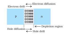
Two important processes occur during the formation of a p-n junction:diffusion and drift.
n-type semiconductor and excess electron while p-type semiconductor has excess holes
During the formation of p-n junction, and due to the concentration gradient across p-, and n- sides, holes diffuse from p-side to n-side (p -> n) and electrons diffuse from n-side to p-side (n -> p). This motion of charge carries gives rise to diffusion current across the junction.
Electron diffusion from n -> p, it leaves behind an ionised donor(positive charge) on n-side which is immobile as it is bonded to the surrounding atoms. As the electrons continue to diffuse from n ? p, a layer of positive charge (or positive space-charge region) on n-side of the junction is developed.
Similarly, hole diffusion from p -> n due to the concentration gradient leaves behind an ionised acceptor (negative charge) which is immobile. As the holes continue to diffuse, a layer of negative charge (or negative space-charge region) on the p-side of the junction is developed.
This space-charge region on either side of the junction together is known as depletion region
This develops an electric field directed from positive charge towards negative charge develops.
Electron on p-side of the junction moves to n-side and a hole on n- side of the junction moves to p-side due to this developed electric field The motion of charge carriers due to the electric field is called drift. Thus a drift current, which is opposite in direction to the diffusion current starts.
The above explained diffusion process continues, the space-charge regions on either side of the junction extend, thus increasing the electric field strength and hence drift current. The process completes when the diffusion current equals the drift current. Thus a p-n junction is formed. In a p-n junction under equilibrium there is no net current.
The loss of electrons from the n-region and the gain of electron by the p-region causes a difference of potential across the junction of the two regions.
this potential tends to prevent the movement of electron from the n region into the p region, it is often called a barrier potential.
Also Read