Question 1
Which one of the following statement(s) is true?
(a)Resistivity of conductors increases with increase in temperature.
(b)Resistivity of semiconductors increases with increase in temperature
(c)Resistivity of semiconductors decreases with increase n temperature.
(d)Resistivity of insulators decreases with decrease in temperature Solution
(a) and (c)
Question 2
The forbidden energy gap Eg in case of semiconductors is of the order of
(a) 6 eV
(b) 1 eV
(c) 0.1 eV Solution
(b)
Paragraph Based Questions
Note: - Question number 3 to 5 are based on the following statement
Certain specimen of metal has $7.87 \times 10^{28}$ free electrons per cubic meter and the mobility of electrons in the metal is 34.8 cm2/Vs Question 3
Conductivity of the metal is
(a) $4.382 \times 10^5$ S/m
(b) $43.82 \times 10^5$ S/m
(c) $438.2 \times 10^5$ S/m
(d) $ .4382 \times 10^5$ S/m
Question 4
If an electric field of 30V/cm is applied across this specimen then drift velocity of free electrons is
(a) 1.044 m/s
(b) 10.44 m/s
(c) .104 m/s
(d) $10.44 \times {10}^2$ m/s
Question 5
Current density for the field applied in question 4 would be
(a) $3.15\times{10}^{10} \; A/m^3$
(b) $3.15\times{10}^{11} \; A/m^3$
(c) $.315\times{10}^{10} \; A/m^3$
(d) $3.15\times{10}^{10} \; A/m^3$ Solution 3-5
Given that mobility of free electrons in metallic specimen is
$\mu=34.8\frac{{cm}^2}{Vs}=34.8\times{10}^{-4}\frac{{\ m}^2}{Vs}$
$Conductivity \sigma=nq\mu=7.87\times{10}^{28}\times1.6\times{10}^{-19}\times34.8\times{10}^{-4}$
$\sigma=438.2\times{10}^5S/m$
Electric field intensity applied across the specimen is
$E=30\frac{V}{m}=30\times{10}^2\frac{V}{m} $
Thus drift velocity of electrons is
$v=\mu E=34.8\times{10}^{-4}\times30\times{10}^2=10.44\ m/s $
And current density is
$J=\sigma E=438.2\times{10}^5\times30\times{10}^2=13.15\times{10}^{10}\ A/m^3 $
Hence the Answer are
3.(c)
4.(b)
5.(a)
Multiple Choice questions
Question 6
Which one of the following statement(s) is/are true?
(a)A substitution impurity in donor and acceptor atoms does not cause any disturbances in the crystal lattice of semiconducting material.
(b)Mobility of charge carriers equals its average speed v divided by the applied electric field E.
(c)Each donor atom contributes two free electrons to semiconducting crystal lattice.
(d)In an n-type semiconductor, the free electrons concentration approximately equals the density of donor atoms Solution
(a),(b) and (d)
Question 7
Donor impurity atoms in semiconducting material results a new
(a)Wide energy band
(b)Narrow energy band
(c)Discrete energy level just below conduction band
(d)Discrete energy level just above valance band Solution
(c)
Question 8
An electron in conduction band
(a) Is located near the top of the crystal
(b) Is bound to its parent atom
(c) Has no charge
(d) Has a higher energy than an electron in the valence band Solution
(d)
Question 9
At zero K (or at absolute zero) the conduction band may be partially filled in
(a) Conductors only
(b) Insulators only
(c) Semiconductors only
(d) Conductors and semiconductors Solution
(a)
Question 10
Good conductors does not have hole current because they are
(a) Full of electrons
(b) Have large forbidden energy gap
(c) Have no valence band
(d) Have overlapping valence band and conduction band Solution
(d)
Question 11
A p-type semiconductor has an acceptor density of 1020 atoms/m3 and intrinsic concentration of 2.5×10¹⁹ m-1 at 300K. The electron concentration in this p-type semiconductor is
(a) $6.23 \times 10^{18}$
(b) $6.25 \times 10^{19}$
(c) $62.5 \times 10^{19}$
(d) $62.5 \times 10^{18}$ Solution
$N_A$ is nearly equal to $n_p$ where $N_A$ is acceptor impurity and $n_p$ is hole concentration.
$n_en_p=n_i^2$
$n_e=\frac{n_i^2}{n_p}=6.25\times{10}^{18}electrons\ per\ m^3$
Hence (a) is the correct answer
Question 12
Mobility of electrons and holes in a sample of intrinsic semiconductors at room temperature are $0.36\ m^2/Vs$ and $0.17\ m^2/Vs$ respectively. If both electrons and hole densities in semiconductor equals $2.5\times{10}^{19}m^3$ then conductivity of semiconducting material is
(a) 212 S/m
(b) 21.2 S/m
(c) 2.12 S/m
(d) .212 S/m Solution
For intrinsic semiconductors
$\sigma=en\left(\mu_e+\mu_n\right)=1.6\times{10}^{-19}\times2.5\times{10}^{19}\left(0.36+0.17\right)=2.12S/m $
Hence (c) is the correct answer
Question 13
Width of depletion region of a pn junction
(a) Is independent of applied voltage
(b) Is dependent on the applied voltage
(c) Is decreased under reversed bias
(d) Is increased under reverse biased Solution
Under reverse biased condition width of the depletion layer is increased because majority charged carriers are pulled away from the junction
hence (b) , (d)
Question 14
Zener breakdown occurs
(a) Mostly in germanium junctions
(b) Due to rupture of covalent bonds
(c) In lightly doped junctions
(d) Due to thermally generated minority carriers. Solution
Zener breakdown occurs in junctions which being heavily doped have narrow depletion region. The breakdown voltage sets up very strong electric field (about 108 V/m) across this narrow layer. This field breaks the covalent bonds which generates the electron hole pairs.
(b)
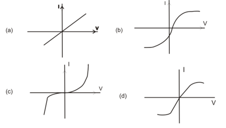
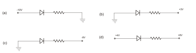
Question 15
The I-V characteristics of a junction diode is of the form Solution
(c)
Question 16
When p-n junction is unbiased, the junction current at equilibrium is
(a) Zero as no crosses the junction
(b) Zero as equal number of carriers crosses the barrier in opposite direction
(c) Mainly due to diffusion of majority carriers
(d) Mainly due to diffusion of minority carriers Solution
For an unbiased pn junction electric current does not flow because drift of minority carriers across the junction is counterbalanced by the diffusion of same number of majority carriers across the junction. These few majority carriers have enough kinetic energy to overcome the barrier and cross the junction. In fact barrier height adjusts itself so that the flow of minority carriers is exactly balanced by the flow of majority carriers across the junction.
Hence (b) is the correct option
Question 17
Consider the following statements regarding the volt-ampere characteristics of pn junction and choose the correct answer using the option given below
1. As the forward applied voltage increases beyond threshold voltage, the forward current rises exponentially.
2. If the forward voltage is increased beyond a certain safe value, it produces an extremely large which may destroy the junction due to overheating.
3. Reverse bias opposes the majority charge carriers to move across the junction.
4. If a reverse voltage is made very high, the covalent bonds near the junction breaks down and large number of electron-hole pairs are librated. Options
(a) Only statements 1 , 2 and 4 are true
(b) Only statements 2 , 3 and 4 are true
(c) Only statements 1 , 3 and 4 are true
(d) Only statements 1 , 2 and 3 are true Solution
(a)
Question 18
If an light emitting diode emits light of wavelength ?=580 nm, then energy gap between valence band and conduction band is
(a) 21eV
(b) 2.1eV
(c) .21eV
(d) .021eV Solution
Given that wavelength of light emitted is
$\lambda=580nm=580\times{10}^{-9}m$
We know that frequency $\nu=c/\lambda$
Or,
$h\nu=\frac{hc}{\lambda} $
$E_g=\frac{hc}{\lambda} $
So, energy gap between valence band and conduction band is
$E_g=\frac{hc}{\lambda}=\frac{\left(6.64\times{10}^{-34}Js\right)(3\times{10}^8\ m/s)}{580\times{10}^{-9}m}=2.1eV $
hence (b) is the correct option
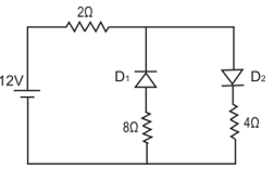
Question 19
Consider the circuit given below which uses two oppositely connected ideal diodes in parallel
The current flowing in the circuit is
(a) 0
(b) .85A
(c) 2A
(d) 1A Solution
The diode D1 is reverse biased and acts as an open switch so there would be no current through D1 and 8O resistor. Diode D2 is forward biased and acts like an closed switch. So current drawn is
$I=\frac{12}{2+4}=2A$
hence (c) is the correct option
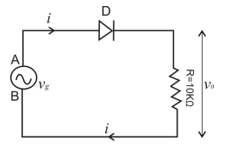
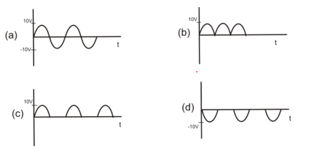
Question 20
Consider the circuit given below
Where voltage source vg generates a sine wave of peak value 10V. Sketch of the wave of voltage v0 across 10K resistor is Solution
We know that a diode conducts only when it is forward biased and here it will conduct only during positive half cycle of input voltage and it will not conduct during the negative half cycle where it is reverse biased.
Since during forward bias, the diode acts as short or a closed switch , the entire generator voltage drops across R. The negative half of vg would be suppressed as in this case diode acts as an open switch.
Hence (c) is the correct option
Question 21
In a full wave rectifier, the current in each diode flows for
(a) the complete cycle of the input signal
(b) half cycle of the input signal
(c) less than half cycle of input signal
(d) zero time Solution
(b)
Question 22
Which of the diodes is/are forward biased in the options given below
Solution
In options (c) and (d) p-type of diode is at higher potential
Question 23
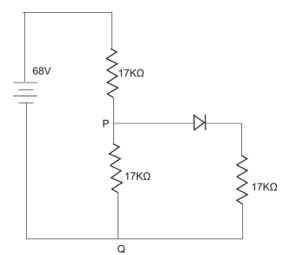
The maximum voltage across points P and Q in the following figure , assuming the diode to be ideal would be
(a) 33.98V
(b) 22.66V
(c) 37.13V
(d) 27.12V Solution
Diode in the circuit is forward biased as p type is at higher potential so diode will acts as a closed switch. Equivalent resistance between point P and Q is
$\frac{1}{R_{eq}}=\frac{1}{17K}+\frac{1}{17K}=0.117 $
So,
$R_{eq}=8500\Omega $
Now for finding out current in the circuit we will have to find total resistance in the circuit and that is
$R=17\times{10}^3+8500 $
$R=25500\Omega$
Current in the circuit is
$I=\frac{V}{R}=\frac{68}{25500}=2.66\times{10}^{-3}A$
Voltage across P and Q is the voltage across $R_{eq}$
$V_{PQ}=IR_{eq}=22.66V$
Hence (b) is the correct option
Question 24
The rectifier efficiencies for half wave and full wave rectifiers are respectively
(a) 35.7% and 71.4%
(b) 30.6% and 61.2%
(c) 40.6% and 81.2%
(d) 39.8% and 79.6% Solution
(c)
Question 25
Consider the following statements about transistors and choose the correct answers using the codes given below
1. The base of transistor is much thinner than the emitter while the collector is wider than both.
2. The emitter is heavily doped so that it can eject large number of carriers into the base.
3. The transistor has two pn junctions i.e., it is like two diodes
4. The resistance of emitter diode is very high as compared to collector diode.
5. The emitter diode is always reverse biased and collector diode is always forward biased. Options
(a) Only 1,2 and 3 are true
(b) Only 2,3,4 and 5 are true
(c) Only 3,4 and 5 are true
(d) 1,2,3,4 and 5 are true Solution
Correct answer is (a)
Question 26
A certain transistor has $\alpha _{dc}=0.98$ and collector leakage current $I_{co}$ equal to $1 \mu A$. If $I_E=1mA$ than collector and base current would be equal to
(a) $.19\mu A$
(b) 19mA
(c) $19\mu A$
(d) .19mA Solution
Given that $I_E = 1mA$
We know that collector current is made up of two parts
(i)Fraction of emitter current that reaches emitter
(ii)Normal reverse leakage current $I_{co}$
Thus,
$I_c=\alpha_{dc}I_E+I_{co}$
Where, $\alpha_{dc}$ is the fraction of emitter current $I_E$ that reaches the collector.
Thus,
$I_c=0.98\times{10}^{-3}+1\times{10}^{-6}=.981mA$
Base current is given as
$I_B=I_E-I_c=19\mu A$
Hence (c) is the correct option
Question 27
For a given emitter current the collector current will be higher if
(a) The recombination rate in the base region were decreased
(b) The emitter region were more lightly doped
(c) The minority carriers mobility in the base region were reduced
(d) The base region were made wider Solution
Due to decrease in the recombination rate in base region more charge carriers reaches the collector region resulting higher collector current.
(a) is the correct option
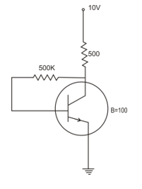
Question 28
Consider the circuit given below
Emitter current in this circuit is
(a) 1.8mA
(b) .18mA
(c) 18mA
(d) .018mA Solution
Here
$I_b=\frac{V_{cc}}{R_b+{\beta R}_c}=\frac{10V}{500\times{10}^3+100\times500}=18\mu A $
Emitter current is given as
$I_E\approx I_c=\beta I_b=100\times{10}^{-6}\times18=1.8mA $
Hence (a) is the correct option
Question 29
Using the information and circuit given in question 4 the collector voltage $V_c$ would be
(a) 91V
(b) 9.1 V
(c) .91V
(d) .091V Solution
Collector voltage
$V_C=V_{CE}=V_{CC}-I_CR_C=10-1.8\times{10}^{-3}\times500=9.1V$
Hence (b) is the correct option
Question 30
The alpha ($\alpha$) of a transistor is its current gain in
(a) Common collector mode
(b) Common emitter mode
(c) Common base mode
(d) Non conducting mode Solution
(c) is the correct option
Question 31
For a pnp transistor to operate in saturation region of its output characteristic in CE configuration which of the following conditions should be met
(a) The emitter base junction should be forward biased and base collector junction should be reversed biased.
(b) Both junctions should be forward biased.
(c) The base emitter junction should be reverse biased and base collector junction should be forward biased.
(d) Both junctions should be reverse biased. Solution
(b) is the correct option
Question 32
Correct relation between $\alpha$ and $\beta$ in a transistor is
(a) $\beta=\frac{\alpha}{1-\alpha}$
(b) $\alpha=\frac{\beta}{1-\beta}$
(c) $\alpha=\frac{\beta}{1+\beta}$
(d) $1+\beta=\frac{1}{1-\alpha}$ Solution
(a) is the correct option
Question 33
In a CB circuit current gain is α=0.92. If emitter current is 1.5mA then base current is
(a) 15mA
(b) 12mA
(c) 0.15mA
(d) 0.12mA Solution
(d) is the correct option
$\alpha _{dc} = \frac {I_C}{I_E}$
or
$I_C= \alpha _{dc} I_E= .92 \times 1.5 \times 10^{-3} = 1.38 \times 10^{-3}$ A
$I_E= I_B + I_C$
$I_B= I_E - I_C= .12 mA$
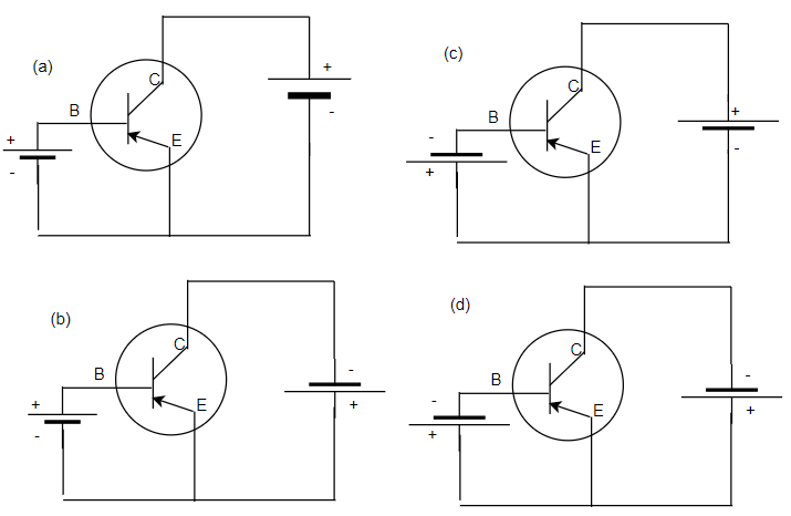
Question 34
Which one of the following diagram shows the correct biasing of the PNP transistor to operate in active region in the CE mode Solution
Answer is (d)
Question 35
A transistor when connected in common emitter mode has a
(a) High input resistance and low output resistance
(b) Medium input resistance and high output resistance
(c) Very low input resistance and a low output resistance
(d) High input resistance and high output resistance Solution
Answer is (a)
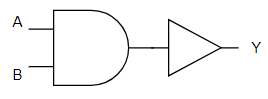
Question 36
The output of the following logic gate is
(a) $Y=\overline{A + B}$
(b) $Y=\overline{A . B}$
(c) $Y=\overline{A} + \overline{B}$
(d) $Y= \overline{A}.\overline{B}$ Solution
Inputs A and B first goes into AND gate and then NOT gate inverts the output of AND gate ,so
$Y=\overline{A . B}$
Hence (b) is the answer
Question 37
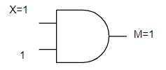
Consider the figure given below
If all the inputs are high ,the value of the output will be
(a) 0
(b) 1
(c) 10
(d) 01 Solution
Output of a OR gate when both the inputs are high will be equal to 1,so
So answer is (b)
Question 38
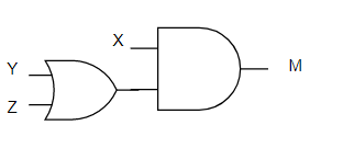
Match List I with List II and select the correct answer using the codes given below
(a) A - 2 , B -3, C-4 ,D-1
(b) A -4 , B - 2 , C -1 , D - 3
(c) A -2 , B - 4 , C -1 , D - 3
(d) A -4 , B - 3 , C -2 , D - 1 Solution
answer is (a)
Question 39
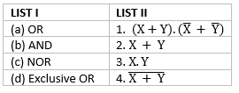
Following truth table represent which logic gate operation
(a) NAND
(b) NOR
(c) NOT
(d) XOR Solution
Answer is (d)
Question 40
An oscillator is nothing but an amplifier with
(a) Large Gain
(b) No feedback
(c) Negative Feedback
(d) Positive feedback Solution

 Solution