Question 1
In a PN-junction diode not connected to any circuit
(a) The potential is the same everywhere
(b) The P-type is a higher potential than the N-type side
(c) There is an electric field at the junction directed from the N- type side to the P- type side
(d) There is an electric field at the junction directed from the P-type side to the N-type side Solution
At junction a potential barrier/depletion layer is formed, with N-side at higher potential and P-side at lower potential. Therefore there is an electric field at the junction directed from the N-side to P-side.
Hence (c) is correct
Question 2
Hole is
(a) an anti-particle of electron.
(b) a vacancy created when an electron leaves a covalent bond.
(c) absence of free electrons.
(d) an artificially created particle Solution
(b)
Question 3
Which of the following statements is not true
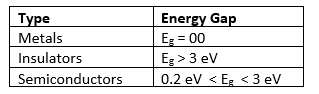
(a) The resistance of intrinsic semiconductors decrease with increase of temperature
(b) Doping pure Si with trivalent impurities give P-type semiconductors
(c) The majority carriers in N-type semiconductors are holes
(d) A PN-junction can act as a semiconductor diode Solution
(c). The majority carriers in N-type semiconductors are holes
Question 4
The conductivity of a semiconductor increases with increase in temperature because
(a) number density of free current carriers increases.
(b) relaxation time increases.
(c) both number density of carriers and relaxation time increase.
(d) number density of current carriers increases, relaxation time decreases but effect of decrease in relaxation time is much less than increase in number density. Solution
(d)
Question 5
The depletion layer in the P-N junction region is caused by
(a) Drift of holes
(b) Diffusion of charge carriers
(c) Migration of impurity ions
(d) Drift of electrons Solution
(b). Due to the large concentration of electrons in N-side and holes in P-side, they diffuses from their own side to other side. Hence depletion region produces.
Question 6
In the depletion region of a diode
(a) there are no mobile charges
(b) equal number of holes and electrons exist, making the region neutral.
(c) recombination of holes and electrons has taken place.
(d) immobile charged ions exist. Solution
(a),(b) and (d)
Question 7
The AC current gain of a transistor is 120. What is the change in the collector current in the transistor whose base current changes by 100 $\mu A$ ?
a. 12 mA
b. 12 $\mu A$
c. 10 $\mu A$
d. 10 mA Solution
(a)
Current gain
$\beta = \frac {\Delta I_C}{\Delta I_E}$
or $\Delta I_E= \beta \times \Delta I_C=120 \times 100= 12$ mA
Question 8
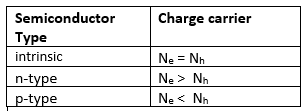
What is the majority charge carrier in p-type semiconductor?
a. Holes
b. electrons
c. Both equal
d. None of the above Solution
(a). Holes are Majority carrier
Question 9
What is relation between power gain, voltage gain and current again of a transistor amplifier?
a. Power gain =Voltage gain/Current gain
b. Power gain =Voltage gain * Current gain
c. Current gain=Power gain * Voltage gain
d. Voltage gain= Current gain/Power gain Solution
(b)
Power gain =Voltage gain * Current gain
Question 10
What is the relationship between current gain $\alpha$ and $\beta$?
a. $\beta = \frac {\alpha}{1 - \alpha}$
b. $\beta = \frac {\alpha}{1 + \alpha}$
c. $\alpha = \frac {\beta}{1 - \beta}$
d. None of the above Solution
(a)
Question 11
Consider an npn transistor with its base-emitter junction forward biased and collector base junction reverse biased. Which of the following statements are true?.
(a) Electrons crossover from emitter to collector.
(b) Holes move from base to collector.
(c) Electrons move from emitter to base.
(d) Electrons from emitter move out of base without going to the collector. Solution
(a), (c)
Question 12
When the P end of P-N junction is connected to the negative terminal of the battery and the N end to the positive terminal of the battery, then the P-N junction behaves like
(a) A conductor
(b) An insulator
(c) A super-conductor
(d) A semi-conductor Solution
(b)
Question 13
In an n-type silicon, which of the following statement is true
(a) Electrons are majority carriers and trivalent atoms are the dopants.
(b) Electrons are minority carriers and pentavalent atoms are the dopants.
(c) Holes are minority carriers and pentavalent atoms are the dopants.
(d) Holes are majority carriers and trivalent atoms are the dopants Solution
(c)
Text Based Questions(long)
Question 1
Explain the following:
(i) In the active state of the transistor, the emitter base junction acts as a low resistance while base collector region acts as high resistance.
(ii)Output characteristics are controlled by the input characteristics in common emitter transistor amplifier.
(iii)LEDs are made of compound semiconductor and not by elemental semiconductors. Solution
(i) Emitter base junction is forward biased whereas base collector junction is reverse biased.
(ii) Small change in the current IB in the base circuit controls the larger current $I_C$ in the collector circuit. $I_C = \beta I_B$
(iii) Elemental semiconductor�s band gap is such that the emitted wavelength lies in IR region. Hence cannot be used for making LED
Question 2
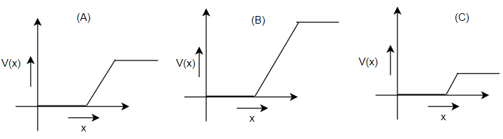
The graph of potential barrier versus width of depletion region for an unbiased diode is shown in A. In comparison to A, graphs B and C are obtained after
biasing the diode in different ways. Identify the type of biasing in B & C and justify your answer. Solution
B : reverse biased
C: forward biased
Question 3
With proper diagram, explain the movement of charge carriers through different parts of the transistor and hence show that $I_E = I_B + I_C$.
Question 4
Draw a circuit diagram to study the input and output characteristics of an n-p-n transistor in its common emitter configuration.
Question 5
Draw the typical input and output characteristics and explain how these graphs are used to calculate current amplification factor of the transistor.
Question 6
Draw the circuit diagram of a full-wave rectifier and briefly explain its working principle.
Question 7
Explain how the depletion layer and barrier potential are formed in a p-n junction diode.
Question 8
Explain how p-n junction diode acts as Half wave rectifier and Full wave Rectifier
Question 9
Define the following terms
(a) Input resistance
(b) Output resistance.
(c) Current amplification factor $\beta$ of a transistor used in its CE configuration.
Short Answer type
Question 1
What is meant by the term doping of an intrinsic semiconductor ? How does it affect the conductivity of a semiconductor ? Solution
Doping of an Intrinsic Semiconductor : The mixing of a small amount of pentavalent (e.g., phosphorus) or trivalent (e.g., aluminium) substance as impurity in a pure semiconductor (e.g., Ge, Si) is called doping.
Doping increases the conductivity of a semiconductor.
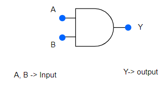
Question 2
Give the logical symbol of an AND gate. Mark the inputs and outputs. Solution
Question 3
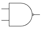
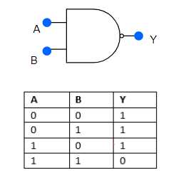
Draw the logic symbol for a NAND gate. Solution
Question 4
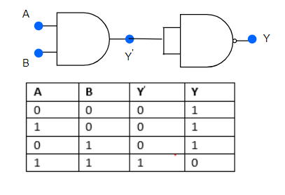
The output of an AND gate is connected to both the inputs of NAND gate. Draw the logic circuit of this combination of gates and write its truth table. Solution
Question 5
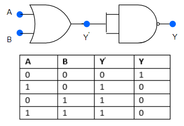
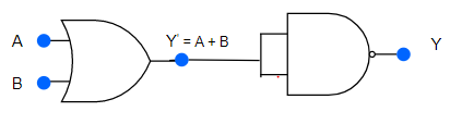
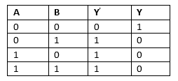
The output of an OR gate is connected to both the inputs of a NAND gate. Draw the logic circuit of this combination of gates and write its truth table. Solution
Question 6
Why are the NAND and NOR gates are known as Universal Gates? Solution
these gates are known as Universal Gates as you can realise other basic gates like OR, AND and NOT from it
Question 7
Write the Full form for the following
a. SSI
b. MSI
c. LSI
d. VLSI
e. IC Solution
SSI -> Small Scale Integration
MSI -> Medium Scale Integration
LSI -> Large Scale Integration
VLSI -> Very Large Scale Integration
Question 8
Draw the energy band diagrams of the below substances
a. Conductor
b. n- type semiconductor
c. p - type semiconductor
d. Insulator
Question 9
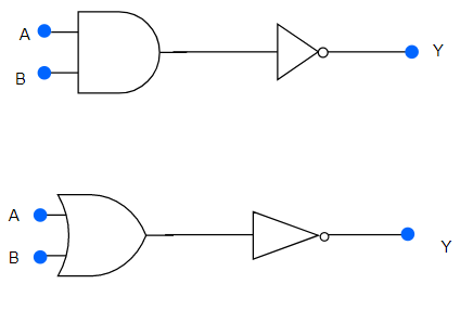
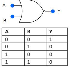
Give the symbol and truth table of each of the two logic gates ,obtained by using the two gate combinations as shown below Solution
a. The gate combination represent a NAND combination
b.The gate combination represent a NOR combination
Question 10
The output of an OR gate is connected to both the inputs of a NAND gate. Draw the logic circuit of the combination of gates and write its truth table Solution
The login circuit of the combination is shown below
And Truth table is